- 您现在的位置:买卖IC网 > Sheet目录1995 > HI5760BIBZ (Intersil)CONV D/A 10-BIT 125MSPS 28-SOIC
5
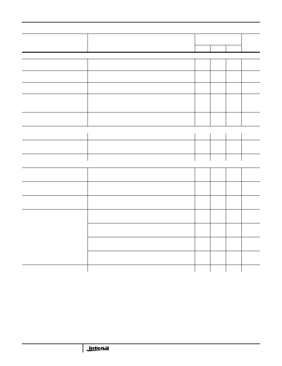
DIGITAL INPUTS
D9-D0, CLK
Input Logic High Voltage with
5V Supply, VIH
(Note 3)
3.5
5
-
V
Input Logic High Voltage with
3V Supply, VIH
(Note 3)
2.1
3
-
V
Input Logic Low Voltage with
5V Supply, VIL
(Note 3)
-
0
1.3
V
Input Logic Low Voltage with
3V Supply, VIL
(Note 3)
-
0
0.9
V
Input Logic Current, IIH
-10
-
+10
A
Input Logic Current, IIL
-10
-
+10
A
Digital Input Capacitance, CIN
-5
-
pF
TIMING CHARACTERISTICS
Data Setup Time, tSU
See Figure 41 (Note 3)
3
-
ns
Data Hold Time, tHLD
See Figure 41 (Note 3)
3
-
ns
Propagation Delay Time, tPD
See Figure 41
-
1
-
ns
CLK Pulse Width, tPW1, tPW2
See Figure 41 (Note 3)
4
-
ns
POWER SUPPLY CHARACTERISTICS
AVDD Power Supply
(Note 8)
2.7
5.0
5.5
V
DVDD Power Supply
(Note 8)
2.7
5.0
5.5
V
Analog Supply Current (IAVDD)
(5V or 3V, IOUTFS = 20mA)
-
23
30
mA
(5V or 3V, IOUTFS = 2mA)
-
4
-
mA
Digital Supply Current (IDVDD)
(5V, IOUTFS = Don’t Care) (Note 5)
-
3
5
mA
(3V, IOUTFS = Don’t Care) (Note 5)
-
1.5
-
mA
Supply Current (IAVDD) Sleep Mode
(5V or 3V, IOUTFS = Don’t Care)
-
1.6
3
mA
Power Dissipation
(5V, IOUTFS = 20mA) (Note 6)
-
165
-
mW
(5V, IOUTFS = 2mA) (Note 6)
-
70
-
mW
(5V, IOUTFS = 20mA) (Note 9)
-
150
-
mW
(3.3V, IOUTFS = 20mA) (Note 9)
-
75
-
mW
(3V, IOUTFS = 20mA) (Note 6)
-
85
-
mW
(3V, IOUTFS = 20mA) (Note 9)
-
67
-
mW
(3V, IOUTFS = 2mA) (Note 6)
-
27
-
mW
Power Supply Rejection
Single Supply (Note 7)
-0.2
-
+0.2
% FSR/V
NOTES:
2. Gain Error measured as the error in the ratio between the full scale output current and the current through RSET (typically 625A). Ideally the
ratio should be 31.969.
3. Parameter guaranteed by design or characterization and not production tested.
4. Spectral measurements made with differential coupled transformer.
5. Measured with the clock at 50MSPS and the output frequency at 1MHz.
6. Measured with the clock at 100MSPS and the output frequency at 40MHz.
7. See ‘Definition of Specifications’.
8. It is recommended that the output current be reduced to 12mA or less to maintain optimum performance for operation below 3V. DVDD and AVDD
do not have to be equal.
9. Measured with the clock at 60MSPS and the output frequency at 10MHz.
Electrical Specifications
AVDD = DVDD = +5V, VREF = Internal 1.2V, IOUTFS = 20mA, TA = 25
oC for All Typical Values (Continued)
PARAMETER
TEST CONDITIONS
HI5760
TA = -40
oC TO 85oC
UNITS
MIN
TYP
MAX
HI5760
发布紧急采购,3分钟左右您将得到回复。
相关PDF资料
HI5762/6IN
CONV A/DDUAL 10BIT 60MSPS 44MQFP
HI5766KCB
CONV A/D 10BIT 60MSPS 28-SOIC
HI5767/6IB
CONV A/D 10BIT 60MSPS 28-SOIC
HI5805BIB
IC ADC 12-BIT 5MSPS 28-SOIC
HI5812JIBZ-T
ADC 12BIT SAMPL TRK&HOLD 24-SOIC
HI5828IN
DAC DUAL 12BIT 130MHZ 48-LQFP
HI5860IBZ
CONV D/A 12-BIT 130MSPS 28-SOIC
HI5960IAZ
CONV D/A 14BIT 130MSPS 28-TSSOP
相关代理商/技术参数
HI5760BIBZ-T
功能描述:数模转换器- DAC D/A 10-BIT 125MSPS 28PIN INDUST TEMP RoHS:否 制造商:Texas Instruments 转换器数量:1 DAC 输出端数量:1 转换速率:2 MSPs 分辨率:16 bit 接口类型:QSPI, SPI, Serial (3-Wire, Microwire) 稳定时间:1 us 最大工作温度:+ 85 C 安装风格:SMD/SMT 封装 / 箱体:SOIC-14 封装:Tube
HI5760EVAL1
功能描述:数据转换 IC 开发工具 HI5760 EVAL PL ATFORM PKG
RoHS:否 制造商:Texas Instruments 产品:Demonstration Kits 类型:ADC 工具用于评估:ADS130E08 接口类型:SPI 工作电源电压:- 6 V to + 6 V
HI5760EVALI
制造商:Harris Corporation 功能描述:
HI5760IA
功能描述:CONV D/A 10-BIT 125MSPS 28-TSSOP RoHS:否 类别:集成电路 (IC) >> 数据采集 - 数模转换器 系列:- 标准包装:2,400 系列:- 设置时间:- 位数:18 数据接口:串行 转换器数目:3 电压电源:模拟和数字 功率耗散(最大):- 工作温度:-40°C ~ 85°C 安装类型:表面贴装 封装/外壳:36-TFBGA 供应商设备封装:36-TFBGA 包装:带卷 (TR) 输出数目和类型:* 采样率(每秒):*
HI5760IA-T
功能描述:CONV D/A 10-BIT 125MSPS 28-TSSOP RoHS:否 类别:集成电路 (IC) >> 数据采集 - 数模转换器 系列:- 标准包装:2,400 系列:- 设置时间:- 位数:18 数据接口:串行 转换器数目:3 电压电源:模拟和数字 功率耗散(最大):- 工作温度:-40°C ~ 85°C 安装类型:表面贴装 封装/外壳:36-TFBGA 供应商设备封装:36-TFBGA 包装:带卷 (TR) 输出数目和类型:* 采样率(每秒):*
HI5760IAZ
功能描述:数模转换器- DAC D/A 10-BIT 125MSPS 28PIN INDUST TEMP RoHS:否 制造商:Texas Instruments 转换器数量:1 DAC 输出端数量:1 转换速率:2 MSPs 分辨率:16 bit 接口类型:QSPI, SPI, Serial (3-Wire, Microwire) 稳定时间:1 us 最大工作温度:+ 85 C 安装风格:SMD/SMT 封装 / 箱体:SOIC-14 封装:Tube
HI5760IAZ-T
功能描述:数模转换器- DAC D/A 10-BIT 125MSPS 28PIN INDUST TEMP RoHS:否 制造商:Texas Instruments 转换器数量:1 DAC 输出端数量:1 转换速率:2 MSPs 分辨率:16 bit 接口类型:QSPI, SPI, Serial (3-Wire, Microwire) 稳定时间:1 us 最大工作温度:+ 85 C 安装风格:SMD/SMT 封装 / 箱体:SOIC-14 封装:Tube
HI5762
制造商:INTERSIL 制造商全称:Intersil Corporation 功能描述:Dual 10-Bit, 60MSPS A/D Converter with Internal Voltage Reference